Source: U.S. National Science Foundation, by Yong Chen, University of Southern California (May 18, 2022). AI-generated summary by biochip.com, published . Not independently reviewed.
Key takeaways
- USC engineers printed microfluidic channels 10 microns high with reported height control of plus or minus one micron.
- The NSF-supported team used vat photopolymerization and a light-blocking platform to keep resin inside channels from curing.
- The work does not report clinical testing, diagnostic accuracy, or commercialization of a finished medical device.
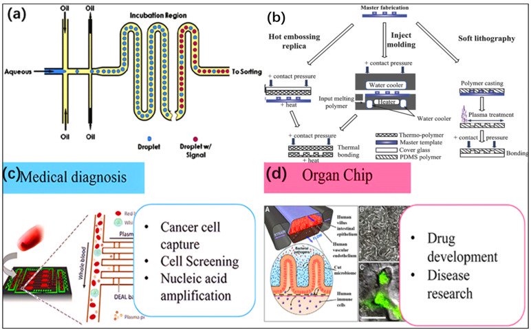
Engineers at the University of Southern California developed a 3D-printing method for making microfluidic chips with channels about 10 microns high, roughly one-tenth the width of a human hair. The National Science Foundation-supported work addresses a stubborn manufacturing problem: tiny fluid channels are useful for biomedical testing but can be labor-intensive to produce. Microfluidic devices guide very small volumes of liquid through patterned channels in a resin chip, much like a miniature plumbing system designed for blood, chemicals, or cells. The USC team used vat photopolymerization, a printing approach that turns liquid resin solid with light. Their process controlled channel height to within plus or minus one micron at the 10-micron scale, Yong Chen said. That precision matters because a channel's dimensions can determine how fluids mix and which cells can move through it. Chen pointed to possible uses in blood testing, including tests for COVID and high blood sugar. The same kind of precisely printed channel could also help separate cells by size before cancer-related analysis.
Why Tiny Channels Are Hard to Make
Microfluidic devices are compact tools built around narrow channels that move, combine, and analyze minute quantities of fluid. In a biomedical setting, a device might carry a blood sample past chemicals that react with a target molecule, producing a signal that can be measured. Because the volumes are so small, the physical dimensions of each channel become central to how the device works.
Making those features reliably is difficult. A channel must have solid walls but remain open inside, which means the material in its interior cannot accidentally harden during fabrication. The smaller the intended gap, the less room there is for error, especially when the target height is only 10 microns.
Using Light to Build an Open Channel
The USC team used vat photopolymerization, a form of 3D printing in which light converts liquid photopolymer resin into a solid. Think of it as selectively shining a lamp into a tank of liquid plastic so that only the illuminated shape hardens. The printer builds the object layer by layer, curing each layer with ultraviolet light and moving the printed object as new layers are added.
The key challenge was limiting how deeply the light cured the resin. Chen explained that the goal is to harden one layer of a channel wall while leaving the resin inside the channel liquid. To accomplish that, the team used a platform between the light source and the printed object to block light from reaching resin that needed to remain uncured.
Controlling Curing at the Microscale
After curing, the remaining liquid resin can be cleared from the channel, leaving an open path through the chip. The team reported channel heights at the 10-micron level with an error of plus or minus one micron. That level of control is important because it gives designers a more predictable way to create structures that handle cells and fluids on a microscale.
The advance is not simply about making a smaller printed object. It is about producing a usable empty space inside a solid resin device without filling that space with accidentally cured material. For microfluidics, the open channel is the working part of the system, just as the hollow pipe is the working part of household plumbing.
Potential Biomedical Uses
Chen described blood testing as one application for such channels. A blood sample could flow through a channel and mix with other chemicals to detect conditions such as COVID or high blood sugar levels. Microfluidic systems are suited to these tasks because they can manage samples and reactions within a compact device rather than requiring large amounts of fluid.
He also highlighted cell separation as a possible use in cancer-related testing. Biopsies remove tissue or an organ sample that can contain both healthy cells and tumor cells. Channels fabricated at accurately controlled heights could separate cells by size, potentially reducing interference from healthy cells before detection.
Why This Matters
Biomedical microfluidic devices depend on geometry as much as they depend on chemistry. A small change in channel height can affect what travels through the device, how materials mix, and whether the chip can distinguish cells of different sizes. A printing method that accurately creates 10-micron channels could therefore give researchers another manufacturing route for devices intended for medical research, drug development, and diagnostic tools.
The next challenge is translating this fabrication control into specific devices and testing how those devices perform with real biomedical samples. The USC technique establishes a way to make finely controlled channels, while its eventual value will depend on how engineers pair those channels with assays, cell-handling steps, and practical testing workflows.
Topics: Microfluidics · Cancer · Diagnostics & precision medicine
Start here: Microfluidics explained
Related articles
- Microfluidic chips: recent advances, critical strategies in design, applications and future perspectives
- Integrated “Lab-on-a-Chip” Microfluidic Systems for Isolation, Enrichment, and Analysis of Cancer Biomarkers
- Multifunctional microfluidic chip for cancer diagnosis and treatment
- Microfluidic biosensors for biomarker detection in body fluids: a key approach for early cancer diagnosis