A research report on lead sulfide (PbS) quantum dots examines how these tiny semiconductor crystals emit light in the near-infrared, a part of the spectrum that is especially useful for imaging, sensing, and telecommunications. Quantum dots are nanometer-scale particles whose optical behavior changes with size, making them attractive building blocks for tunable devices. In this study, the authors focus on a wide range of particle diameters rather than a narrow, idealized subset, which matters because real-world synthesis often produces nanocrystals with meaningful size variation. By analyzing photon emission across that broader size window, the work helps clarify how crystal size shapes color, efficiency, and emission dynamics. That makes the findings relevant not only to basic nanoscience but also to engineers trying to design better detectors, light sources, and biomedical probes. PbS is particularly important because it emits in the near-infrared at sizes that are relatively straightforward to make in the lab. The result is a more practical picture of how these nanocrystals behave when translated from theory into actual materials and devices.
What the study set out to measure
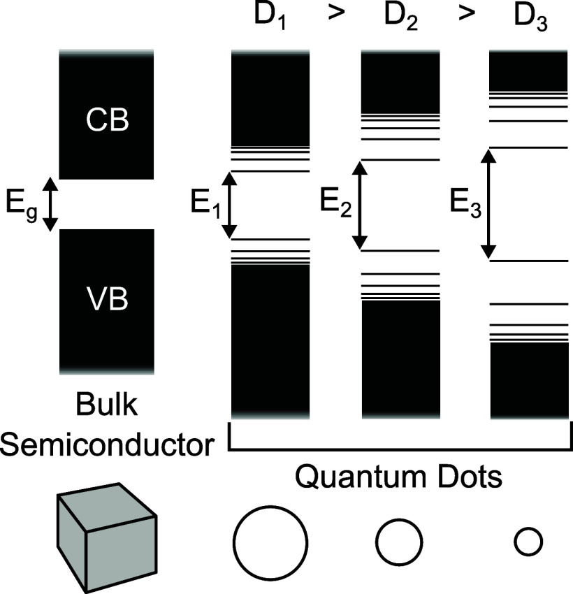
The core question is simple: how do PbS quantum dots emit photons when their diameters span a large range? In quantum dots, size is not a minor detail; it directly affects the energy levels available to electrons and holes, the positively charged absence left behind when an electron is excited.
When an electron and hole recombine, they can release that energy as a photon, producing light. Because smaller quantum dots confine charges more tightly, they generally emit at shorter wavelengths, while larger dots shift emission toward longer wavelengths in the near-infrared.
Why PbS quantum dots are special
PbS has become a widely studied material because its electronic structure is well suited for near-infrared emission. That spectral region is valuable because near-infrared light can travel through some materials, including biological tissue and optical fibers, better than visible light in certain situations.
The material also offers strong size-dependent tunability, which means researchers can adjust emission simply by controlling nanocrystal diameter during synthesis. That makes PbS a versatile platform for studying how nanoscale structure translates into measurable optical behavior.
A broader diameter range gives a more realistic picture
Many laboratory studies examine a limited set of highly uniform particles to isolate clean physical effects. This work stands out by looking across a larger diameter range, which is closer to how nanocrystal batches often appear in practice.
That broader approach matters because size dispersion, meaning variation in particle size within the same sample, can widen emission peaks and complicate interpretation. By treating the diameter range as a central feature rather than experimental noise, the study helps bridge the gap between elegant theory and manufacturable materials.
What photon emission reveals about quantum confinement
The emission behavior of quantum dots is governed by quantum confinement, the effect that emerges when a crystal becomes so small that charge carriers are restricted in their motion. In bulk semiconductors, electrons can occupy bands of energies, but in quantum dots those energies become more discrete, more like steps than a ramp.
As the dot size changes, the spacing between these allowed energies changes too. Measuring emitted photons therefore provides a direct readout of how confinement evolves across different nanocrystal diameters, offering a way to map structure onto function.
Implications for device design
Understanding emission over a large size range is useful for anyone trying to build an application around PbS nanocrystals. Devices such as infrared LEDs, photodetectors, and optical sensors all depend on predictable relationships between particle size, emission wavelength, and radiative performance.
If those relationships hold only for narrow, carefully selected samples, they are less helpful in industrial settings. Data that capture realistic size distributions can improve material selection, guide synthesis targets, and make device behavior easier to reproduce from one batch to the next.
Challenges beneath the signal
Photon emission from quantum dots is not determined by size alone. Surface chemistry, defects, particle-to-particle interactions, and the surrounding environment can all influence whether excited states release energy as light or lose it through non-radiative pathways, which means the energy disappears as heat instead of photons.
That is one reason studies like this are valuable even when the main variable is diameter. Looking across a broad set of nanocrystals can expose where simple size-based models work well and where other factors begin to dominate the optical response.
Why This Matters
This kind of measurement work may sound specialized, but it feeds directly into technologies people increasingly depend on. Near-infrared nanocrystals could improve low-cost imaging systems, expand optical communication components, and support biosensors that detect disease markers with light rather than bulky instrumentation.
Just as importantly, the study adds practical knowledge to the field of nanomaterials. Instead of assuming every sample is perfectly uniform, it addresses the variability that scientists and manufacturers actually have to manage, which is often where promising materials either succeed or fail outside the lab.
What comes next
The next step for this line of research is to connect emission trends more tightly to synthesis methods, surface passivation strategies, and device architectures. Surface passivation, a technique that coats or chemically stabilizes the quantum dot surface, is especially important because it can suppress defects that quench light emission.
If researchers can combine precise size control with better surface engineering, PbS quantum dots may become more reliable components in commercial infrared technologies. Studies that map optical behavior across realistic particle populations are likely to remain essential, because they provide the kind of grounded understanding needed to turn nanocrystals from fascinating lab materials into dependable products.