A team led by researchers at the University at Buffalo has designed a tiny reusable sensing chip that could help push point-of-care testing into a more sensitive and practical next phase. The work addresses a frustrating tradeoff in modern biosensors: engineers can build extremely small nanostructures that are good at detecting molecules, but those same structures can be so cramped that molecules struggle to reach the places where detection happens. To get around that problem, the researchers created a layered chip that uses microscopic cavities and a droplet of liquid gallium to guide molecules into the sensing region while also strengthening the optical signal. The device operates with surface-enhanced infrared absorption, or SEIRA, a method that reads the infrared light absorbed by molecules to identify what is present in a sample. In simple terms, the chip is designed to make it easier both to catch target molecules and to see them clearly. That combination matters because many rapid medical tests depend on sensors that can work with tiny sample volumes, deliver results quickly, and avoid expensive laboratory equipment. If the approach continues to perform well, it could support a new generation of compact diagnostic tools for clinics, emergency settings, and possibly home use. Just as important, the sensor is reusable, which could help reduce cost and waste in future testing platforms.
The bottleneck in ultra-small sensors
Point-of-care tests have become a familiar part of medicine, from glucose meters to rapid infectious disease screens. Their appeal is simple: they bring testing closer to the patient, reducing the need to send samples to centralized labs and wait hours or days for answers.
But improving the sensing technology inside those tests is not easy. Many cutting-edge optical sensors rely on nanostructures, features so small they are approaching the scale of the molecules they are trying to detect, and that creates a design problem. Smaller structures can intensify light and improve sensitivity, but they can also make it physically harder for molecules to enter the sensing zone in the first place.
A sensor built like a tiny sandwich
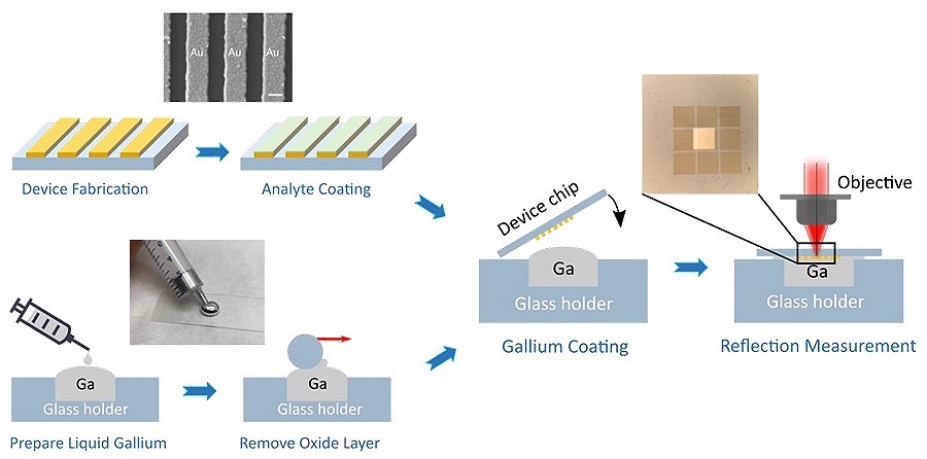
The Buffalo-led team tackled that challenge with a layered design. According to the university's description, the researchers formed a sandwich-like structure using patterned layers, a drop of liquid gallium as the base, and a thin glass cover on top.
That architecture creates what the team calls a nanopatch antenna. In optics, an antenna of this kind is a nanoscale structure that concentrates electromagnetic energy into very small spaces, allowing weak molecular signals to become easier to measure. Here, the cavities in the chip help funnel molecules into the right locations while also trapping enough infrared light to analyze the sample.
How SEIRA helps read molecules
The sensing method at the heart of the device is surface-enhanced infrared absorption spectroscopy. Infrared light is useful because many molecules absorb specific infrared wavelengths based on their chemical bonds, giving them a kind of spectral fingerprint.
SEIRA boosts that effect by placing molecules near specially engineered surfaces that amplify the local electromagnetic field. When that happens, the molecule's infrared signature becomes much easier to detect, even in very small quantities. For medical testing, that can be valuable because biomarkers, measurable signs of disease or health status, are often present at very low concentrations.
Why liquid gallium is interesting
One especially notable part of the design is the use of gallium, a metal that can be liquid near room temperature depending on conditions. Liquid metals are attractive in microscale devices because they can conform to structures in ways rigid materials cannot.
In this sensor, the gallium serves as the base layer while helping create the optical conditions needed for the nanopatch antenna to work. That may sound like a subtle materials choice, but it points to a broader engineering strategy: instead of only shrinking structures further, the team rethought how geometry and materials could be combined to improve access for molecules and preserve sensitivity.
The people behind the work
The project was led by Peter Q. Liu, an assistant professor of electrical engineering at the University at Buffalo School of Engineering and Applied Sciences. He worked with Xianglong Miao, a PhD candidate in his lab, and Ting Shan Luk at the Center for Integrated Nanotechnologies at Sandia National Laboratories.
The study was published in Advanced Materials in January, indicating that the work has passed peer review and entered the scientific literature. University research announcements often highlight broad potential before a technology reaches market, but publication in a major materials journal suggests the underlying device concept is being taken seriously by the field.
Why reusability matters
Many diagnostic chips are designed for one-time use, which makes sense for contamination control but can also drive up cost. A reusable sensor could be attractive in settings where the sensing surface can be cleaned or regenerated while the rest of the system remains intact.
That matters most for decentralized testing, where budgets, supply chains, and waste disposal can all be limiting factors. A chip that combines strong sensitivity with repeat use could make advanced optical testing more realistic outside large hospital laboratories.
Why This Matters
This research matters because it addresses a practical problem that often gets overlooked in flashy nanotechnology headlines: a sensor is only useful if real samples can reliably reach the active region. The Buffalo team's design tries to solve that access problem without giving up the sensitivity benefits of nanoscale optics.
If successful, the concept could support tests for disease biomarkers, chemical exposure, or other medically relevant targets using very small amounts of fluid. That aligns with a larger trend in healthcare toward faster, more portable diagnostics that can be used at the bedside, in urgent care clinics, or eventually at home.
What comes next
As with many early-stage sensor advances, the next steps will likely involve proving performance with real biological samples, testing durability across repeated use, and integrating the chip into complete diagnostic systems. Building a clever sensing surface is only one part of the challenge; researchers also need robust sample handling, calibration, and manufacturing methods.
Still, the work offers a clear example of how small changes in structure can unlock bigger gains in usability. Rather than simply making nanosensors smaller and more complex, this team focused on making them more accessible to the molecules they need to measure, a practical insight that could help shape the next wave of point-of-care testing.