Source: Polymers, written by Chan Hee Kim; Hae Woon Choi; Jong Hyun Kim (October 7, 2026). AI-generated summary by biochip.com, published . Not independently reviewed.
Key takeaways
- Keimyung University researchers used near-field electrospinning to pattern PEO fiber molds for closed PDMS microfluidic channels.
- Changing voltage from 1.4 to 1.9 kilovolts controlled fiber widths from about 34 to 100 micrometers.
- The work does not establish performance in a specific biosensing assay or clinical application.
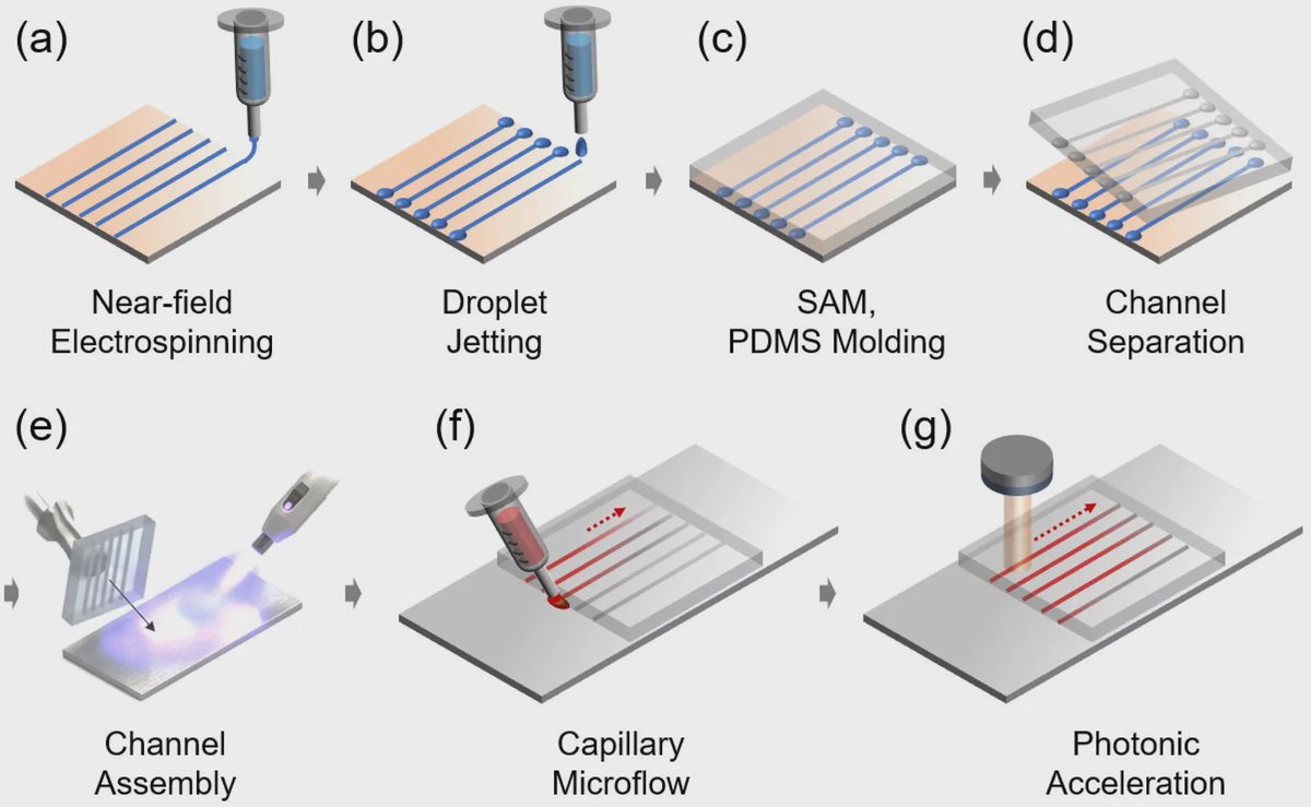
Researchers at Keimyung University developed a way to make polymeric microfluidic channels using patterned polymer fibers instead of the photomasks and cleanroom-made master molds commonly used in chip fabrication. The approach uses near-field electrospinning to directly write polyethylene oxide fibers onto a silicon wafer, then transfers their shape into transparent polydimethylsiloxane, or PDMS. By adjusting the spinning voltage from 1.4 to 1.9 kilovolts, the team controlled fiber widths from about 34 to 100 micrometers. The resulting closed channels moved aqueous liquids without a pump, suggesting a lower-complexity route for prototyping capillary-driven lab-on-a-chip devices.
Writing a Mold With Fibers
Near-field electrospinning, or NFES, draws very fine polymer fibers from a needle using an electric field. It works a bit like using a computer-controlled glue gun, except the deposited strands are tens of micrometers wide and serve as temporary raised features rather than the final device.
The Keimyung University team dissolved polyethylene oxide, or PEO, in deionized water and deposited the material onto a silicon wafer. A programmable XY stage moved the collector beneath the needle, allowing the researchers to place straight fiber lines and reservoir-dot patterns along defined paths.
Those fibers became a mold base for PDMS, a transparent silicone material widely used in microfluidics. After surface treatment, the team cast PDMS over the fiber pattern, replicated the geometry, and bonded the PDMS structure to glass following ultraviolet-ozone treatment. This created enclosed microchannels without conventional photolithography or a separate master mold.
Voltage Sets Channel Dimensions
The electric field was a key control point. Increasing the NFES voltage within the tested 1.4 to 1.9 kilovolt range allowed the researchers to tune fiber width from approximately 34 to 100 micrometers, producing semi-elliptical channel cross-sections in the replicated PDMS.
That control matters because channel geometry influences how fluids behave at small scales. In a capillary channel, surface tension can pull liquid forward without external pumping, much as a paper towel draws up spilled water. The shape and dimensions of the channel alter the curvature of the liquid interface, which changes the pressure driving that movement.
Capillary Flow Without a Pump
The team used theoretical calculations and numerical analysis to examine this effect. As channel width decreased, the liquid interface became more curved and the calculated capillary driving pressure increased. The analysis predicted faster flow velocity and greater capillary filling in narrower channels.
Experiments with aqueous solutions confirmed spontaneous transport in the fabricated devices. The researchers also reported that light-induced modulation enhanced flow acceleration and reversal, showing that the channels could support forms of non-powered flow control beyond passive filling.
Why This Matters
Microfluidic chips handle tiny liquid volumes for tasks such as sample delivery, chemical analysis, and biosensing. Conventional PDMS microfluidics often begins with photolithography, a process that can require cleanroom equipment, photomasks, and a newly fabricated master mold whenever the channel design changes.
Using directly written PEO fibers as a reusable mold base could make design changes more straightforward: a revised channel layout can be programmed into the motion of the deposition stage rather than requiring a new photomask. The method retains PDMS, an optically transparent material familiar in lab-on-a-chip research, while replacing a major fabrication step.
The next practical question is how consistently this fiber-based process can produce more complex channel networks and how it performs in specific sensing or biological assays. Still, the work establishes NFES-patterned fibers as a controllable template for rapidly making capillary microfluidic structures.
Topics: Lab-on-a-chip · Microfluidics
Start here: Microfluidics explained
Related articles
- Microfluidics-based strategies for molecular diagnostics of infectious diseases
- Microfluidic-based biosensors toward point-of-care detection of nucleic acids and proteins
- Doroth Raises US$4.5 Million to Build Latin America’s First Microfluidic Chip Plant
- Next generation microfluidics: fulfilling the promise of lab-on-a-chip technologies