Source: Biosensors, by Teodora Despotovski Kiš; Marko Radović; Brankica Kartalović; Nikola Knežević (September 6, 2026). AI-generated summary by biochip.com, published . Not independently reviewed.
Key takeaways
- BioSense Institute researchers reviewed recent porous silicon biosensors for bacteria, biomolecules, and viruses using optical and electrochemical readouts.
- Electrochemical etching can tune porous silicon pore morphology through current density, electrolyte composition, etching duration, illumination, and wafer doping.
- Reproducible fabrication, structural stability, surface oxidation, and scalable device integration remain unresolved challenges for porous silicon sensors.
Researchers at the BioSense Institute, University of Novi Sad, have reviewed how electrochemically etched porous silicon can serve as the active material in optical and electrochemical biosensors. The review compares recent sensor designs for bacteria, biomolecules, and viruses, including devices combined with microfluidic systems and lab-on-a-chip formats. Porous silicon matters because its tiny, controllable pores create a large reactive surface while retaining the optical and electrical behavior of silicon. The field's central challenge is turning those attractive material properties into sensors that can be fabricated consistently and remain stable in practical use.
A Silicon Sponge for Biosensing
Porous silicon, often shortened to pSi, begins as a crystalline silicon wafer. Electrochemical etching removes material from the wafer in a controlled way, creating a network of nanoscale or microscale pores. A useful analogy is a sponge made from a semiconductor: its internal surfaces give molecules many places to interact, while its silicon framework can transmit optical or electrical signals.
Researchers can tune the pore size, pore density, layer thickness, and surface chemistry by changing the etching current density, electrolyte composition, etching time, illumination, and wafer doping. Those fabrication choices determine whether the resulting material is microporous, mesoporous, or macroporous, and they shape the sensor's final performance.
How Electrochemical Etching Forms Pores
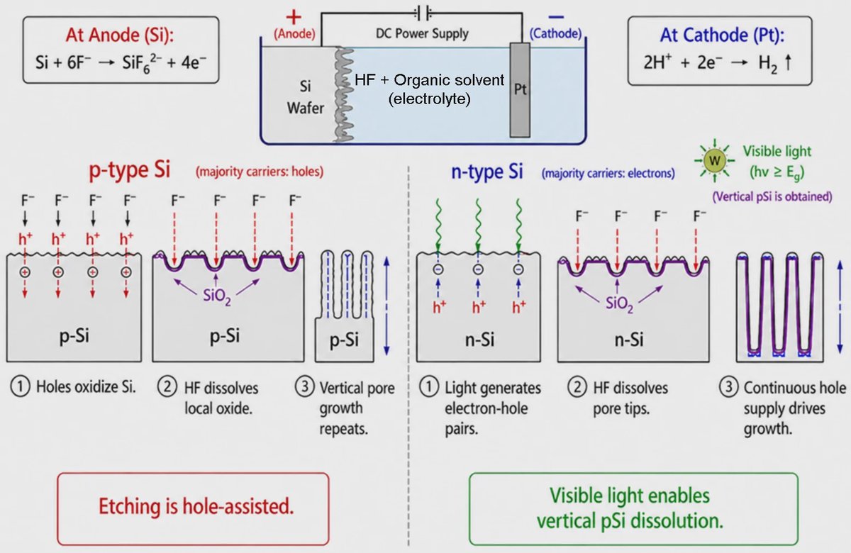
In electrochemical etching, the silicon wafer acts as the anode in a hydrofluoric acid-based electrolyte. Applying a voltage drives reactions that dissolve silicon at selected locations, and fluoride ions help carry away the dissolved material. The local availability of positively charged carriers called holes helps determine where pores begin and how they grow.
The process differs for p-type and n-type silicon, which contain different electrically active dopants. P-type silicon can form pores under anodic bias without light because holes are readily available at the surface. N-type silicon generally needs illumination, high voltage, or heavy doping to supply holes, and light can confine pore formation to illuminated regions for micropatterning.
Small variations in dopant distribution, surface defects, electric-field concentration, and hydrofluoric acid transport can steer pore formation. That sensitivity is useful for engineering structures, but it also creates a manufacturing problem: devices require reproducible pore networks if they are to produce repeatable measurements.
Two Ways to Read a Biological Signal
Optical pSi sensors detect changes in light. When a target molecule binds inside or on the porous layer, it can alter the material's refractive index, meaning the way it bends and reflects light. Sensors may read that change through reflection, transmission, scattering, interferometric signals, photonic structures, or fluorescence from quantum dots incorporated into pSi.
Electrochemical sensors instead measure an electrical response associated with chemical reactions or charge transfer at the porous surface. Because pSi is semiconducting and electrochemically active, it can support signal amplification and charge-transfer processes. Both approaches rely on adding a recognition layer, such as an antibody, enzyme, nucleic acid, or aptamer, that preferentially captures the intended target.
Surface Chemistry and Faster Transport
The freshly etched material provides silicon-hydrogen and silicon-hydroxyl surface groups, creating sites for chemical modification. Coatings based on metals, polymers, graphene derivatives, and biomolecular recognition layers can improve selectivity, sensitivity, and stability. These modifications help turn a porous material into a sensor aimed at a specific bacterium, biomolecule, or virus.
Getting a sample into the pores quickly is another major design issue. Molecules moving only by diffusion can take time to penetrate a complex porous network, much as water moves slowly into a dense sponge. The review highlights microfluidic and lab-on-a-chip integration as a way to manage fluid flow, reduce mass-transfer limitations, shorten response times, and potentially lower detection limits.
Why This Matters
Porous silicon could support low-cost, adaptable sensing platforms because it combines a high surface area with established silicon microfabrication methods. That makes it compatible with miniaturized and multiplexed devices, where several targets could be measured within a compact system. Potential applications span clinical diagnostics, environmental monitoring, food safety, and biomedical research.
But the material's promise depends on solving persistent practical problems. The review identifies reproducible synthesis, structural stability, surface oxidation control, and scalable device integration as priorities for future work. Progress will depend on connecting etching conditions, pore structure, surface chemistry, fluid handling, and signal readout into robust sensor designs.
Topics: Biosensors · Lab-on-a-chip · Microfluidics
Start here: Microfluidics explained