Source: Sensors (Basel, Switzerland), written by Hongjun Gu; Junhan Chang; Jintao Su; Meiling Zhang; Xue Li; Jing Zhou; Lixin Hou (October 14, 2026). AI-generated summary by biochip.com, published . Not independently reviewed.
Key takeaways
- The simulated sensor reached 1,127 nm/RIU sensitivity and a 0.45 RIU detection range.
- Its double-slot trapezoidal grating design uses envelope tracking and achieved simulated mode-conversion efficiency above 95 percent.
- The study used numerical simulations and does not establish performance in a fabricated, experimentally tested sensor.
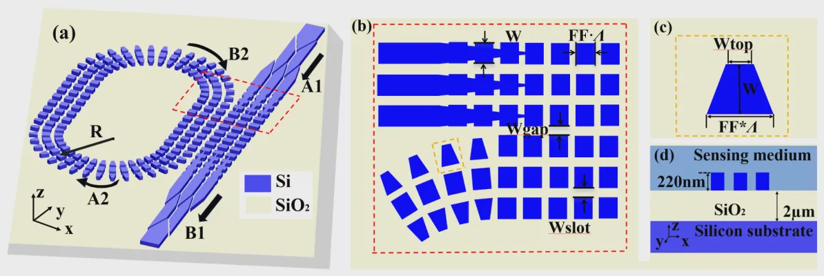
Researchers at Jilin Agricultural University and Jilin University have proposed a silicon photonic sensor designed to measure refractive-index changes across a much wider range than conventional microring sensors. The device combines a double-slot waveguide with trapezoidal subwavelength gratings and tracks the movement of a broad spectral envelope instead of following a single resonance peak. In computer simulations, that approach produced a detection range of 0.45 refractive-index units and a sensitivity of 1,127 nanometers per refractive-index unit. The results suggest a way to combine sensitive measurements with a broader operating range in a compact optical sensing platform.
A ring designed to interact with its surroundings
A micro-ring resonator is a loop-shaped optical circuit that traps light, creating a pattern of resonances that shifts when the material around the ring changes. The team’s design adds a double-slot structure, which directs more of the optical field into the spaces where an analyte, the substance being measured, can interact with it. Greater overlap between light and analyte can make changes in the surrounding refractive index easier to detect.
The ring and its bus waveguide use subwavelength gratings, or SWGs: repeating structures with features smaller than the wavelength of the light traveling through them. These repeating patterns can shape how light moves through a waveguide. In the curved sections of the ring, the silicon grating blocks have trapezoidal profiles, a geometry the researchers designed to improve optical confinement and reduce scattering loss.
The proposed sensor is designed for a silicon-on-insulator platform with a 220-nanometer silicon layer and a 2-micrometer buried oxide layer. Transitions between different waveguide sections are handled by three mode converters: strip-to-slot, slot-to-double-slot, and double-slot-to-SWG. Simulations put their average conversion efficiency above 95 percent.
Following the spectrum’s envelope
Conventional microring sensors often measure how far one resonance peak shifts. That method runs into a limit: when the peak moves beyond the resonator’s free spectral range, or FSR, it can become unclear which resonance is being tracked.
The team instead proposes following the overall envelope of the sensor’s spectrum, a broad outline formed by its resonances. Think of it as following the shape of a wave rather than trying to keep track of one ripple. Because the envelope shifts as the surrounding refractive index changes, the researchers say it can provide an unambiguous measurement beyond the single-peak FSR limit.
What the simulations found
Using a 2.5-dimensional finite-difference time-domain method, a computer simulation technique for modeling how light moves through a structure, the researchers estimated a refractive-index sensitivity of 1,127 nanometers per refractive-index unit (RIU). They also reported a concentration sensitivity of 2,780 picometers per percent and a simulated detection range of 0.45 RIU.
The modeled device had a quality factor of 1,885, a measure related to how sharply defined its resonances are, and an extinction ratio of 15.7 decibels, which describes the contrast between transmission levels in the spectrum. The researchers calculated a theoretical limit of detection of 8.87 × 10⁻⁶ RIU. That figure is a model-based estimate, not a reported measurement from a physical sensor.
Why This Matters
Many sensing applications need a device to detect small changes without losing track of measurements over a wider range. The proposed combination of stronger light-analyte interaction and envelope tracking addresses both challenges in simulation, and the researchers identify lab-on-a-chip sensing as a potential application.
The study reports numerical modeling, not experimental validation of a fabricated device. Testing whether the design can be built and deliver the simulated performance in practice remains an important next step.
Start here: Biosensors explained
Related articles
- Graphene Oxide Microfiber Aptasensor for Neutrophil Monitoring
- Integrated Microfluidic CRISPR Diagnostic Device for Rapid HPV Testing
- Miniaturization of Aptasensors in Organic Electrochemical Transistors for Sensitivity Enhancement
- From Device-Level Implementation to In-Sensor Computing in Memristive-Device-Based Biosensors: A Review